Focus on automotive semiconductor production, SBI Holdings and PSMC's new semiconductor plant

🟦SBI to establish semiconductor plant with PSMC in Taiwan “25 regions are being selected as candidates”
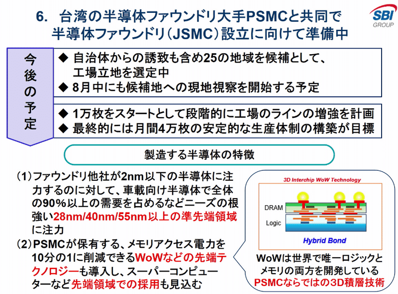
SBI Holdings is considering establishing a domestic semiconductor plant with Taiwanese semiconductor foundry PSMC (Helix Accumulation Electron Manufacturing) Japan. Twenty-five regions have been selected as candidates for plant locations, and we have been invited by local governments. Production at the new plant will start with a monthly production of 25,1 wafers, and eventually aim to produce 4,<> wafers per month.
🟦 Targeting the semi-advanced semiconductor market with strong needs
The new plant targets the semi-advanced semiconductor market, where there is a strong need. By focusing on the semi-advanced areas of 28nm, 40nm and 55nm processes, we are targeting 90% of the automotive semiconductor market. While advanced foundries such as TSMC are focusing on semiconductors below 2nm, this semi-advanced process-specific approach will create differentiation.
In the new process, we plan to produce packaging technology, which is a post-process. We will introduce “WoW” (10D stacking technology), an advanced technology possessed by PSMC that can reduce memory access power by one-tenth. This package technology is expected to be used not only in automotive semiconductors but also in supercomputers, which are more advanced technologies.
“WoW”(Wafer-on-Wafer)”
It is a 3D stacking technology for semiconductor chips that directly stacks two wafers. The semiconductor devices on each wafer are connected to form a single integrated circuit. This technology streamlines communication between devices and significantly reduces memory access power.
🟦Summary
Focusing on automotive semiconductor production, a semi-advanced semiconductor market with strong needs, SBI Holdings and PSMC’s new semiconductor plant
PSMC, which has strengths in DRAM manufacturing, probably wants to utilize “WoW” using DRAM.

