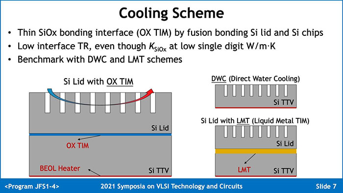
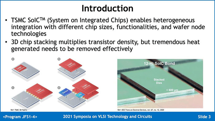
TSMC gave a lecture at the VLSI symposium on the technology to directly water cool the chip itself.

🟩 Higher chip density
The smaller the chip and the more heat is generated in a semiconductor, the higher the density of heat and the harder it is to cool. As semiconductor processes evolve and circuit density increases, 3D packaging (a technology that stacks chips vertically) advances, and heat dissipation has become an important chip cooling issue.
TSMC is considering this as a solution to direct the coolant to the chip.

🟩 Why do you need direct water cooling of the chip?
Currently, data centers sometimes use water cooling as a means of cooling nVIDIA and Intel chips that generate several hundred watt heat. The higher the heat density, the more difficult it is to cool, so it is not easy to handle waste heat in the range of several hundred W in a small area such as a chip.
TSMC’s goal is to develop a cooling technology of 10 W (10 W/mm²) per square millimeter. Although it depends on the size of the chip, a 500 mm² chip will have 2000 W class cooling, so it is a very high target.
🟩Summary
The reason for TSMC’s research on chip water cooling is that it is aimed at increasing the integration density of chips
Semiconductors have been highly integrated by Moore’s Law, but various approaches have been taken with an eye on Morethan Moore. Not only the chip, but also the technology to mount and cool the chip is also key. We also have high hopes for the development of 3D packaging technology in Japan.

