Taiwan Semiconductor Manufacturing Co., Ltd. (TSMC) is considering a shift from the originally planned 6~7 nanometers (nm) to a more advanced “4 nanometer” process for its second plant under construction in Kikuyo Town, Kumamoto Prefecture, and it has been found that there is a change in construction trends.
TSMC mulls making more advanced chips at 2nd Japan plant to feed AI boom
🟧TSMC Kumamoto Plant 2 Planning Review and Changes in Construction Trends
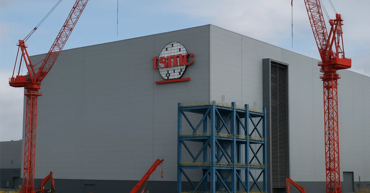
Taiwan Semiconductor Manufacturing Co., Ltd. (TSMC) is building its second plant (JAIM Plant 2) in Kikuyo Town, Kumamoto Prefecture. Initially, the factory was mainly intended for manufacturing logic semiconductors with a circuit width of 6~7 nanometers, but it is reported that they are considering switching production to a more advanced “4 nanometer” process against the backdrop of a surge in demand for advanced technologies such as for AI (artificial intelligence) data centers.
- Review of production targets
Initially, the company planned to focus on 6nm to 7nm, but it is reported that it is also considering advanced processes in the 4nm class. This is a strategic decision to respond to the growing demand for high-performance chips for AI. - Movement at the construction site At the site of the second plant, which started construction in
October, a large number of cranes and heavy machinery were in operation until around November, but the number has decreased sharply since then, and there is information that there will be no equipment introduction in 2026. This has spread the view that “construction is temporarily suspended”. - Impact on the start of operation Regarding the
scheduled start of operation in 2027, it has been pointed out that there is a possibility of extending the schedule due to design reviews and policy changes.
🟧 Why is the shift to “4 nano” attracting attention?
The nanometer (nm) of a semiconductor is a measure of the circuit width, and the smaller the number, the finer and more high-performance the process. Conventional 6~7nm processes have been widely used in smartphone SoCs and automotive semiconductors, but the 4nm class is becoming mainstream for high-performance processors for generative AI and large-scale data centers. For this reason, TSMC’s review of its plans for the second Kumamoto plant is due to changes in the market environment, with global demand for AI rapidly increasing.
There is also a view that chips for AI and high-performance computing (HPC) require high EUV (extreme ultraviolet exposure) equipment and packaging technology, which may require optimization of factory design and equipment specifications. As a result, the change of plan can be seen as a strategy to increase flexibility in the competition of manufacturing technologies.
🟧 Conclusion
TSMC Kumamoto Plant 2 is likely to be strategically redesigned from a 6-7nm plan to 4nm manufacturing, and the movement of construction sites is also changing. This reflects a global trend that responds to the growing demand for AI and data centers.
In Japan, in addition to TSMC, Micron is promoting EUV mass production of advanced DRAM in Hiroshima, and Rapidus is taking on the challenge of developing EUV-based development with next-generation logic. If multiple factories that actually handle EUV are set up and the number of engineers who experience processes, equipment, and yields increases, it is expected that semiconductor productivity and technology absorption capacity in Japan as a whole will further increase.