Through a new licensing agreement with Metalenz in the United States, STMicroelectronics will establish a mass production system for its next-generation optical technology “Metasurface” and aim to expand its applications from smartphones to automobiles.
🟦 ST Micro Strengthens Partnership with Metalenz to Accelerate Mass Production of Metasurface Optics
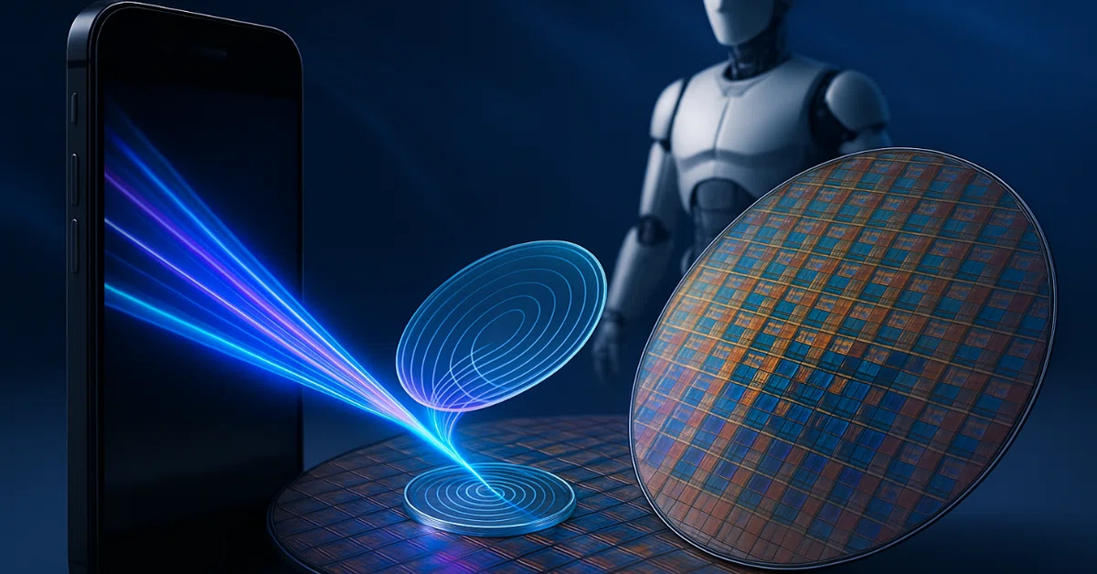
STMicroelectronics announced a new licensing agreement with Metalenz, a U.S.-based metasurface technology company. Under this agreement, ST will leverage Metalenz’s intellectual property (IP) and leverage its proprietary manufacturing base to launch full-scale mass production of Metasurface optics. This is expected to significantly expand the range of applications from consumer to automotive and industrial sectors.
- ST leverages its unique production technology that combines 300mm semiconductor wafers with optical fabrication
- Metalenz IP for a wide range of applications, including biometrics, LiDAR, and gesture recognition
- Meta-optics is also used for the FlightSense module, which has already shipped more than 140 million units
🟦 The key to the spread of metasurfaces is “semiconductorization” and “high-precision mass production”
The background of this announcement is the industry’s need for increased sophistication and miniaturization of optical components. Especially in the smartphone and automotive fields, there is a need to improve sensor performance and save space in products, and conventional lens structures have seen their limitations.
Metasurface optics is a new technology that allows light to be controlled with ultra-thin structures instead of thick lenses, and Metalenz is a pioneer in this technology. ST has already had a significant track record of implementing this technology in 2022 and aims to expand further with this agreement. ST’s strength is that it can realize the concept of “making optics using a semiconductor process” ahead of its competitors.
🟦 Summary
The strengthening of the partnership between ST and Metalenz is expected to significantly advance the mass production and practical application of metasurface optics.
The mass production of cutting-edge optical technology within the framework of semiconductor manufacturing is likely to further accelerate the evolution of sensing and recognition functions.

