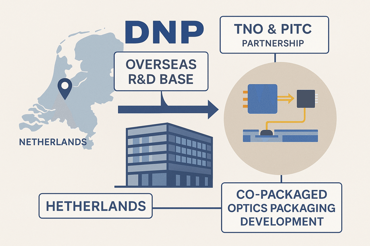
DNP will establish a new R&D center in Eindhoven, the Netherlands, which is a European advanced technology base, to accelerate the development of package components for next-generation semiconductor technology “photoelectric fusion”.
Opening of the first overseas R&D center in the Netherlands | News | DNP
🟦DNP opens a research center for photoelectric fusion packaging materials in the Netherlands
Dai Japan Printing (DNP) has announced the establishment of its first overseas R&D base at its “High-Tech Campus” in Eindhoven, the Netherlands. His research theme is the development of packaging materials for semiconductors related to “photoelectric fusion” technology, which has been attracting attention in recent years. First, three Japan researchers will be stationed in the field to conduct research in collaboration with local institutions.
- At the new base, we will develop “precision patterning technology for optical materials” for semiconductor package components using photoelectric fusion over a three-year period.
- In collaboration with the Netherlands Organization for Applied Science (TNO) and the optical chip research organization PITC, we will integrate advanced European technology with DNP’s materials technology.
- We are also looking at developing partner companies and forming an innovation network in Europe.
🟦 Optoelectronic convergence is the key to supporting next-generation communication infrastructure
With the spread of generative AI and the expansion of cloud use, data centers are experiencing a surge in information transmission and power consumption. To address this, “Co-Packaged Optics” technology, which utilizes optical signals instead of electrical signals, is attracting attention. DNP has always had strengths in microfabrication such as photomasks and functional films, and we decided that it could play an important role in the development of new semiconductor packaging materials that integrate light and electricity.

In Europe, advanced semiconductor companies such as Intel, ASML, and NXP are concentrated, and the high-tech campus Eindhoven is its core base. With DNP based here, we have a system in place to be involved in the development of global technical rules.
🟦 Summary
DNP will accelerate the development of packaged components at its European research sites to support next-generation communication technologies that combine light and electricity.
In the increasingly sophisticated semiconductor industry, not only chips but also “packages” are becoming more important. Especially in technologies that fuse electricity and light, such as photoelectric fusion, precise packaging materials are essential.


