OKI and Nisshinbo Micro Devices have jointly developed a 3D analog IC used in ADAS (Advanced Driver Assistance Systems), and have succeeded in reducing the size of the IC by more than 30% and suppressing noise compared to conventional systems.
🟦New Possibilities Realized by OKI and Nisshinbo 3D Analog ICs
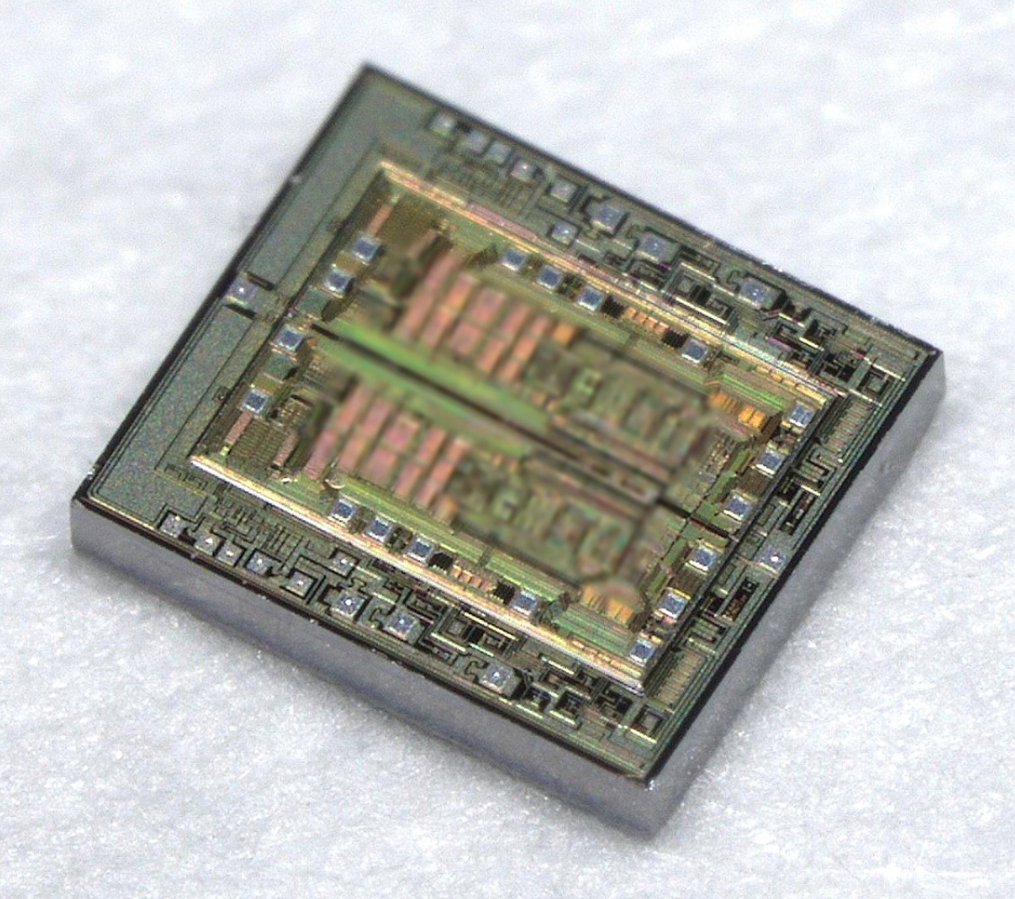
The 3D analog IC developed by OKI and Nisshinbo Micro Devices is made by stacking different chips on a substrate to improve functionality and achieve a size of more than 30% compared to conventional products. In particular, it is expected to be used in automotive ADAS, etc., and will be used for signal processing in cameras, sensors, and LiDAR. This, in turn, is expected to further accelerate the adoption of ADAS.
🟦 Why Miniaturization and Noise Suppression Succeed
The reason for the success in miniaturization and noise suppression of 3D analog ICs is the combination of OKI’s CFB technology and Nisshinbo Microdevice’s local shielding technology. In CFB technology, the bonding between the chips is performed only by intermolecular forces, and interference between devices is minimized by not using adhesives. In addition, the stripped, thin ICs are only a few micrometers thick and can be connected using a redistribution layer, resulting in a denser integration.
🟦Summary
The 3D analog ICs developed by OKI and Nisshinbo Micro Devices will improve performance and reduce the size of ADAS, accelerating innovation in the automotive market. Mass production is scheduled for 2026, which will have a significant impact on the market in the future.
The specific product for this 3D analog IC has not yet been decided, but I feel that the effect of the technology will be even more effective when the target application is clear, such as the multilayer technology for Sony’s image sensors.