DNP begins full-scale development of 2nm generation photomasks for EUV exposure
🟦 Dai Japan Printing begins full-scale development of photomask manufacturing process for 2nm generation logic semiconductors
DNP (Dai Japan Printing) has begun full-scale development of a photomask manufacturing process for 2nm generation logic semiconductors. It is compatible with EUV exposure, which is the most advanced technology in semiconductor manufacturing.
- EUV exposure: Exposure technology using extreme ultraviolet rays, which enables finer circuit formation than conventional ArF
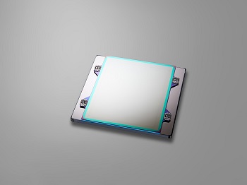
- Photomask: An original plate for transferring semiconductor circuit patterns with light
DNP will participate as a subcontractor in NEDO’s “R&D Project for Strengthening the Infrastructure of Post-5G Information and Communications Systems,” in which Lapidus Inc. is participating. We aim to complete development by FY2025 and start mass production at the Kamifukuoka Plant in Saitama Prefecture in FY2027.
🟦 Leading the world in photomask technology
In recent years, cutting-edge logic semiconductors have been produced using EUV lithography. In 2016, DNP became the first manufacturer specializing in photomasks to introduce a multi-electron beam mask lithography system, and has strengthened its response to semiconductor manufacturing in advanced areas with high productivity and quality.
In addition, we have started development with an eye on the 2nm generation and beyond, and have signed an agreement with imec, a cutting-edge international research institute headquartered in Belgium, for the joint development of photomasks for next-generation EUV.
🟦Summary
DNP has begun full-scale development of a photomask manufacturing process for 2nm generation logic semiconductors that supports EUV lithography, which is the most advanced process in semiconductor manufacturing. We aim to complete development by FY2025 and start mass production in FY2027.
DNP has announced that it will acquire Fujitsu’s subsidiary, Shinko Electric, and is actively investing in the semiconductor field. This is a move that symbolizes the transformation of the printing industry.