🟩 Led by the Japanese government?
Sony declined to comment, but said that “in general, stable procurement of semiconductors is important for maintaining Japan’s competitiveness.”
TSMC does not normally collaborate in this way, but there is a possibility that it will be realized because of inquiries from the Japanese government.
🟩 Candidate construction site
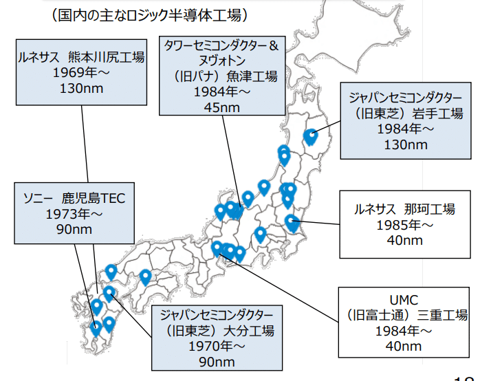
Sony’s image sensor factory in Kumamoto is a candidate
The land and plant will be handled by Sony, and the manufacturing process will be handled by TSMC.
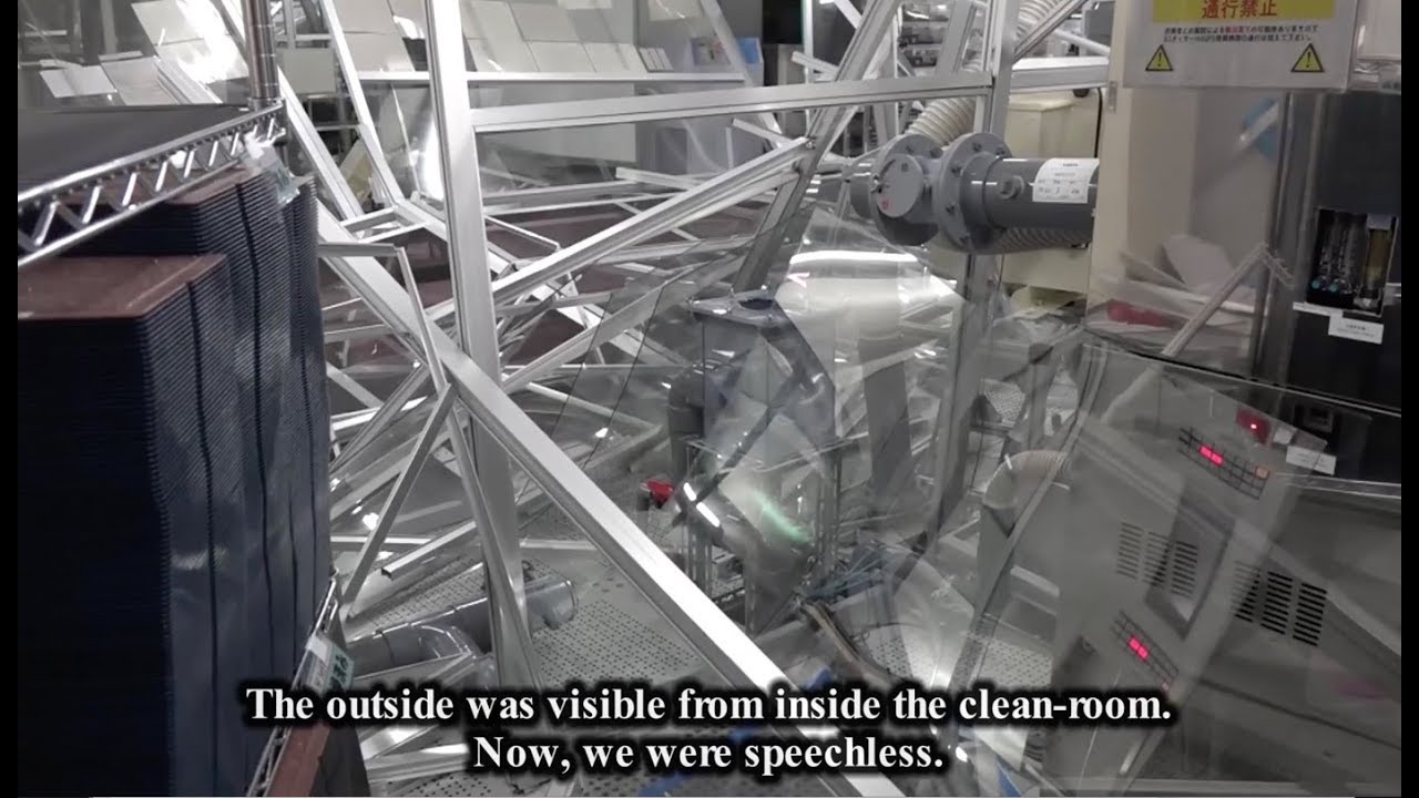
By the way, this Sony Kumamoto factory was greatly damaged by the 2016 Kumamoto earthquake
🟩 Relationship between Sony and TSMC
From 2020, Sony image sensors are produced in the TSMC40nm process
TSMC Begins Production Preparations for Sony CMOS Image Sensor – Taiwan Media CoverageTSMC is preparing to purchase the necessary new equipment and certify it for the production of Sony’s high-end CMOS image sensor products.news.mynavi.jp
It is said that it is also looking at manufacturing with the next-generation 28nm process.
🟩 Advanced process?
In Japan, we are planning to use the most advanced 20nm process.
Looking at the world, 5nm that has been mass-produced since 2020 is the latest
Even though it is 20 nm, it is already a process several generations old.
🟩Summary
Although it is not state-of-the-art, the reason why semiconductor factories are returning to Japan is
Good things for the accumulation of supply chains and technologies, I would like to expect