Samsung Electronics held the Samsung Foundry Forum 2021 online
🟩 Samsung Electronics Announces Advanced Semiconductor Process Roadmap
Samsung Electronics has announced that it will start production of 3nm process chip designs in the first half of 2022. In 2023, we will release an improved version of 3nm. The 3 nm process reduces area by 35 percent, improves performance by 30 percent, or consumes 50 percent compared to the 5 nm process. Current yields are approaching a level similar to that of the 4nm process. Beyond that, the advanced 2nm process is in the early stages of development and will be produced in volume production in 2025.
As for 2nm, TSMC, the leader in the foundry industry, has not stated the timing of mass production.
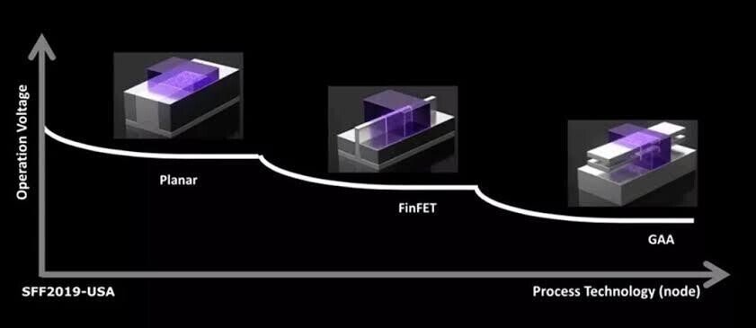
🟩 Adoption of transistor structure
Samsung has announced the adoption of a new MBCFET (Multi-Bridge Channel Field Effect Transistor) structure for its 3nm process. This is commonly referred to in the industry as a GAA (Gate All Around) structure. In the case of Intel, it is called RibbonFET, but the basic structure is the same. The integration of FinFET, which is the current mainstream advanced process transistor structure, is becoming limited. Therefore, advanced processes are expected to shift to a GAA structure.
Samsung Electronics is trying to highlight the technological capabilities of semiconductor foundries by mass-producing the new process with the new structure of GAA.
🟩Summary
Samsung Electronics is using a new structure of transistors for its 3nm process to promote the technological capabilities of semiconductor foundries.
The only companies that can manufacture advanced processes are TSMC in Taiwan, Samsung Electronics in South Korea, and Intel in the United States. It is very sad that there are no names of companies Japan electronic nation.