🟩NAND TO MORE THAN 100 LAYERS OF 3D STRUCTURE
IN THE PAST, NAND MEMORY WAS A TWO-DIMENSIONAL STRUCTURE IN WHICH TRANSISTORS CONSTRUCTED ON CHIPS WERE MINIATURIZED TO INCREASE THE INTEGRATION. HOWEVER, IT HAS HIT THE LIMIT OF MINIATURIZATION, AND SINCE AROUND 2006, WE HAVE BEEN ADOPTING A THREE-DIMENSIONAL STRUCTURE THAT IS STACKED VERTICALLY. THANKS TO THIS, THE STORAGE DENSITY OF NAND FLASH MEMORY HAS BEEN INCREASING ALMOST TWICE AS FAST AS IT HAS BEEN ALMOST TWO YEARS SINCE 2006.
🟩KEY PLAYERS IN NAND MEMORY
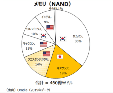
- Samsung Electronics
- Kioxia-Western Digital Camp
- SK Hynix
- Micron
SK HEINIX ACQUIRED THE INTEL NAND BUSINESS UNIT IN 2020, AND THERE ARE FOUR MAJOR PLAYERS IN NAND MEMORY WORLDWIDE.
🟩 the latest generation of each company
IN THE NAND INDUSTRY, IT WILL BE DIVIDED INTO THIRD GENERATION (32 LAYERS), FOURTH GENERATION (64TH AND 72ND LAYER), FIFTH GENERATION (92, 96 LAYERS), AND SIXTH GENERATION (128 LAYERS) DEPENDING ON THE NUMBER OF LAYERS. IT USUALLY TAKES ABOUT A YEAR OR TWO TO EXCEED A GENERATION.
samsung electronics
Since 2020, the multilayer NAND Flash “V-NAND” has achieved 128 layers in the latest sixth generation, achieving a capacity of 512Gb (gigabit) with TLC.
In the second half of 2021, the company will release the 7th generation 176-layer V NAND V-NAND. In addition, Samsung electronics says it has already completed the prototype of an eight-generation VNAND with more than 200 layers.
micron
Micron Technology will begin mass production and shipped the world’s first 176-layer 3D NAND flash memory in 2020.
kioxia
Kioxia, a former Toshiba memory company, announced flash memory using a three-dimensional laminated structure for the first time in the world in 2007. It has been announced that it has developed a 162-layer 6th generation 3D NAND flash memory in collaboration with Western Digital Corporation of “BiCS FLASHTM”
, which has been in mass production since 2020, applying the fifth generation 112-layer lamination process.
SK HYNIX
SK Hynix announced the completion of the development of a 176-layer 512 Gigabit (Gb) triple-level cell (TLC) 4DNAND flash in 2021. The development of a 176-stage NAND flash memory was the second after Micron, a U.S. semiconductor company.
YMTC (NAGAE YUSHIRO SCIENCE AND TECHNOLOGY)
IN 2021, CHINESE MEMORY SEMICONDUCTOR COMPANY YMTC (YANGTZE YUSASHI TECHNOLOGY) BEGAN MASS PRODUCTION OF 128-LAYER 3D NAND FLASH MEMORY PRODUCTS. AT THE END OF 2018, THE COMPANY FLEW 64 AND 96 LAYERS AND IMMEDIATELY ENTERED THE DEVELOPMENT OF 128 LAYERS, AND DECLARED THAT MASS PRODUCTION WOULD BEGIN AT THE END OF 2020.
🟩 summary
NAND MEMORY’S LATEST TECHNOLOGY IS 160-176 LAYERS OF 3D NAND
NAND is probably thanks to the efforts of research developers to overcome the various difficulties that have evolved into 2D-> 3D in order to increase integration. Semiconductors continue to evolve and will continue to evolve in accordance with Moore’s Law.
Thank you for watching. Please share if you like!