Samsung Electronics of Korea starts mass production of next-generation advanced semiconductors
🟦 Samsung Electronics 3nm process mass production begins.
Samsung Electronics has started mass production of 3nm process products using a new transistor structure. Samsung began mass production at its Hwaseong plant in South Korea, and its customer is said to be an ASIC fabless manufacturer in China.
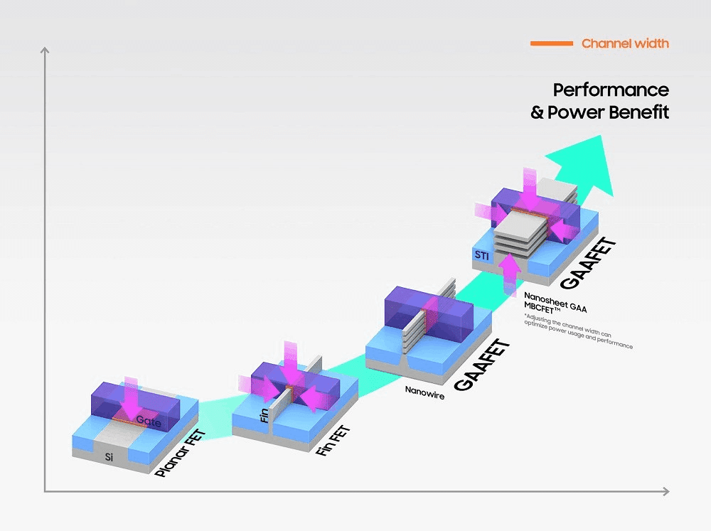
GAA structure
Samsung Electronics has mass-produced the world’s first GAA (gate-all-around) transistor process. TSMC plans to mass-produce 3nm process semiconductors with conventionally structured transistors later this year. The 3nm process was mass-produced by Samsung about half a year earlier. However, in the semiconductor industry, simple comparisons are not possible because the naming rules of processes differ depending on the company. Since it uses GAA, Samsung looks better in performance compared to the previous life 5nm.
3nm process (5nm ratio)
Performance Power consumption
Samsung 23% 45%TSMC 10~15% 25~30%
🟦 TSMC Strengthens Foundry Business
Samsung Electronics is rushing to develop advanced technologies and will chase TSMC, the world’s leader in the field of semiconductor contract manufacturing. Both companies occupy the top two positions in the field of semiconductor contract manufacturing. However, TSMC’s share is more than 2%, and the gap between the two companies is large, with Samsung in second place with 50%. Samsung Electronics is actively introducing advanced processes to strengthen its foundry business. Samsung’s aggressive adoption of new technologies took time to get yields on track from the start of mass production even when introducing 2nm.
🟦Summary
Samsung Electronics Foundry Business Starts Mass Production of Next-Generation Advanced Semiconductors to Chase TSMC
Samsung Electronics actively introduces new technologies and takes risks.